Announcement of the Death of Arthur Jericke
> read moreGIN-TTL Digital Interface
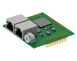
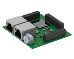
✓ 60 freely configurable GPIOs
✓ Universal, flexibel and economical
✓ With Pins or sockets strips available
The GIN-TTL is a universally applicable digital I/O module. The card has 60 inputs or outputs with LVCMOS level. With the standard firmware, 60 freely configurable GPIOs are available. Additional functions can be built in through customer-specific FPGA firmware; e.g. interrupt inputs and outputs. The GIN-TTL module is a very flexible and cost-effective interface between existing third-party devices and the GinLink.
Digital 3,3V inputs / outputs: | |
Number of inputs / outputs | 60 |
I/O signaling standard | LVCMOS |
Voltage level | 3,3 V |
Max. output current per output | 4 mA |
Output circuit | Tri-State |
FPGA: | Xilinx Spartan6 |
Dimenions | with pins 60x60x25 mm (LxWxH) |
Logic power supply: | |
Voltage | 3,3 VDC ± 10 % |
Power consumption (min / typ / max) | 180 /250 / 350 mA |

